
Design Of Electronic Switch Using Transistor
Normally the function of a switch is either turning on or off close path of current flow and carry current at any direction. If there were no switches, we would have to disconnect or connect every time from main power supply whenever we need to turn off or on light, fan etc. These are all mechanical switches which mechanically disconnect appliances from main power supply.
BJT(Bipolar Junction Transistor) is a solid state electronic switch which can perform switching operation without mechanically disconnected. It is the great invention in the field of electronics. This solid state switch is used for
- Controlling high power devices like motors, solenoids , Relays etc.
- Digital electronics and logic gate circuits and many others.
By observing a microcontroller model atmega32 datasheet, I found, it can provide maximum current of 40mA at guaranteed operating condition. So when we need to Run a relay(requires about 80mA current) DC motor(Requires more than 150mA current) what is the solution????
Then BJT is the simplest and low cost solution as I found from study.
How to design BJT as a electronic switch?
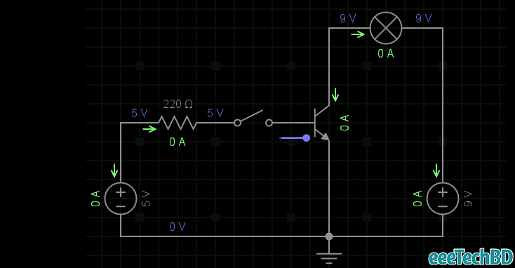
Before we start our main discussion, let’s see the schematic how I control a dc motor using 5 voltage pulse(Microcontroller pulse) but motor(In circuit motor is indicated by yellow light) is originally powered up by a 9 voltage battery.
For my convenience I guess, you know the basic operating principal of BJT,how it works and you solved BJT related problems but right now you don’t know how to design circuit using BJT to solve your real life problem.
Some basic discussion regarding BJT
if you have the basic idea regarding cut-off mode and saturation mode you can skip fundamentals and go to DESIGN PROCEDURES.
Output characteristic of BJT is given below.

We know BJT works in three region
- Cut-off region
- Saturation region
- Active region
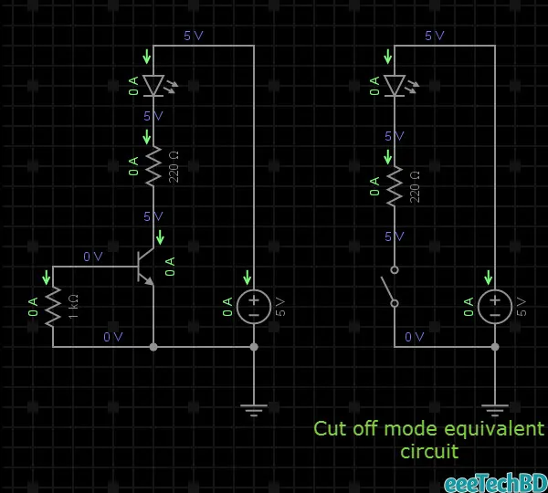
Cut-off mode characteristic
- BJT is fully off
- Emitter-Base voltage Vbe<0.7 , So Emitter-Base Junction is reversed biased
- Collector-Base Junction is also reverse biased
- Zero base and collector current
- Collector Emitter voltage Vce will be high or maximum
As a result in cut-off mode BJT works as a open switch just given below.
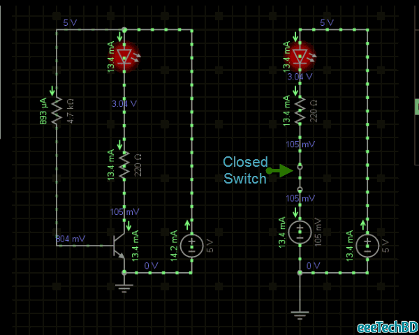
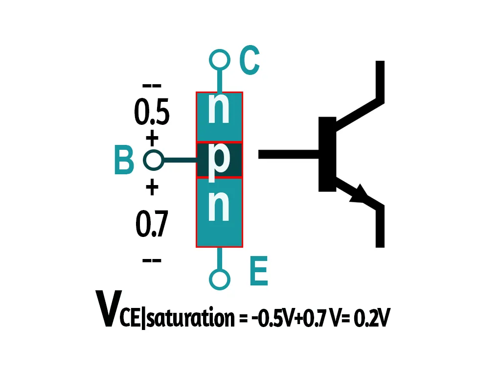
 Saturation Mode characteristics
- BJT is fully on
- Maximum base and collector flows( depletion layer decreses)
- Collector emitter voltage is minimum (100mV to 300mV). In diagram 134mV
- Emitter-base and collector Base junction are forward biased.
As a result The Transistor works as a Closed switch given below.
N.B:
In both cut-off and saturation mode BJT dissipates minimum power.
So now one thing is clear that using cut-off mode and saturation mode behavior we can use BJT as a SPST switch
Design Procedures:
Now we start our main discussion on How you precisely design BJT as a switch for your project.
Design Cut-off Mode:
Designing Transistor as cut-off mode is very simple. When any high current device(Motor, Solenoid, Relay) is running under BJT switch just make Vbe< 0.5(EBJ and CBJ are reversed biased) or connect the base with ground.
Design Saturation mode
BJT will go to saturation when Emitter-Base and Collector Base junction are forward biased. It is a little bit tricky to design BJT in saturation mode. We need to Increase Base voltage sufficiently large enough for collector Base junction to become forward biased and transistor leave the active region and enters the saturation region.
We know BJT is not symmetric, So voltage drops different for two forward biased junctions are as follow.
EOS (Edge of saturaion) = This is the critical point between active region and saturation region.
Before start our design we need to focus our problems and requirements.
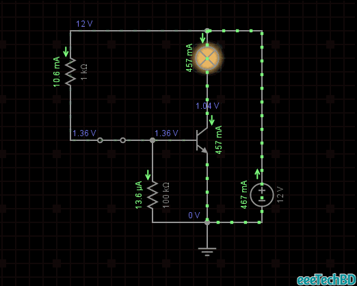
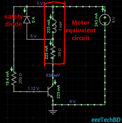
We will run a 6V DC motor motor which equivalent circuit resistance is 20ohms and requires 230mA curent to operate in the rated condition.
So we need to operate the BJT in saturation region so that it can supply maximum current.
STEP 1:
Calculate the Collector current assuming the Transistor in saturation mode. We know, in saturation mode Collector to emitter voltage is 0.2v . Using this voltage value we can calculate edge of saturation(EOS) collector current.
In our design we use PN2222 transistor. Click here to download datasheet.
which is less then our transistor model PN2222’s collector current. It can handle 600mA of collector current
STEP 2:
Calculate Base current from collector current. So we need minimum beta which we find from manufacture datasheet. For PN2222 transistor minimum Dc current gain beta is 100
This is the minimum base current which keeps the transistor at the edge of saturation region. If we increase the base current more by a factor, we are driving the Transistor further into saturation. The factor is known as Overdrive factor(ODF).
\[ODF = \frac{I_B}{I_{B(EOS)}}\]We let ODF=10 which means we are forcing the transistor go deep into saturation 10 times than edge of saturation.
\[I_B = ODF \times I_{B(EOS)}\] \[= 24mA\]STEP 3:
The standard format of the preceding circuit is given below. Now we calculate Base resistor Rb value so that the transistor stays saturation mode.
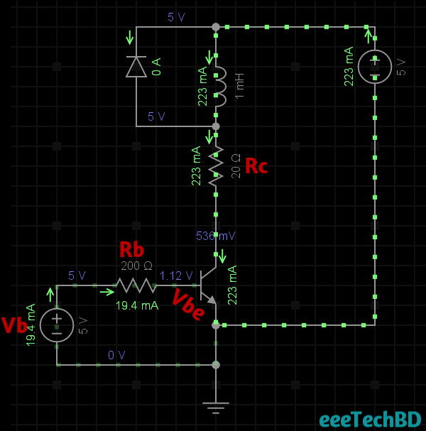
Nearest available value for Rb is 200 Ohm.
In the simulation we notice that all the values are close to our calculated value. So design is complete.
Checking Saturation region:
No we will check whether the transistor is operating in the saturation region or not.
If transistor operates in the saturation region, then saturation mode Dc current gain will be much less than Active mode minimum DC current gain .
As Beta is much less than Active mode minimum beta, so our design is perfect and the transistor is operating in the saturation region.
Leave a comment